new website for Xccela Consortium -
developing new local bus for embedded memoryfication chips
Editor:-
October 4, 2018 - A new website to support a new
storage ORG was
announced
today. The Xccela Consortium (at
www.xccela.org) now has 12 member companies working to promote the Xccela Bus as
an open-standard digital interconnect and data communications bus suitable for
volatile and nonvolatile memories as well as other types of ICs.
new thinking in SSD controller techniques reveals "layer
aware" properties exploitable in 3D nand flash
Editor:- June
30, 2018 - A new twist using
RAID ideas in
SSD controllers has
surfaced recently in a research paper -
Improving
3D NAND Flash Memory Lifetime by Tolerating Early Retention Loss and Process
Variation (pdf) by Yixin Luo and Saugata Ghose (Carnegie Mellon
University), Yu Cai (SK Hynix), Erich F. Haratsch (Seagate Technology) and
Onur Mutlu (ETH Zürich) - which was presented at the recent
SIGMETRICS conference
June 18-22, 2018.
The new RAID is called Layer-Interleaved RAID (LI-RAID) -
which the authors say "improves reliability by changing how pages are
grouped under the RAID error recovery technique. LI-RAID uses information about
layer-to-layer process variation to reduce the likelihood that the RAID recovery
of a group could fail significantly earlier during the flash lifetime than the
recovery of other groups." ...
read the article (pdf)
Editor's comments:- the new RAID is
just one of many gems in this research paper. Others being the discovery that
remanence in 3D nand includes a significant short term charge loss (in the first
few minutes after writes), and also that an endurance based characterization of
a small part of each chip can be used to predict an optimized layer dependent
threshold read voltage for all the layers in the chip. I've discussed the
significance of adding the concept of "layers" to "number of raw
chips" to the thinking in SSD controller design in my recent
home
page blog.
ReRAM based architectures for Processing-In-Memory (guide)
Editor:-
May 1 , 2018 - Processing in memory and ReRAM are both making their mark
independently as noteworthy technologies which each promise new fashions in
the shape of future memory systems design. But how about combining both?
A
new paper -
A
Survey of ReRAM-Based Architectures for Processing-In-Memory and Neural Networks
(pdf) by Sparsh
Mittal, Assistant Professor at Indian Institute of Technology
Hyderabad summarizes the state of art.
In his abstract Sparsh says "As
data movement operations and power-budget become key bottlenecks in the design
of computing systems, the interest in unconventional approaches such as
processing-in-memory (PIM) and machine learning (ML), especially neural network
(NN) based accelerators has grown significantly. ReRAM is a promising
technology for efficiently architecting PIM and NN based accelerators due to its
capabilities to work as both: high-density/low-energy storage and in-memory
computation/search engine. In this paper, we present a survey of techniques for
designing ReRAM-based PIM and NN architectures. By classifying the techniques
based on key parameters, we underscore their similarities and differences."
...read
the article (pdf)
Spin Transfer Technologies says its breakthrough tweak to MRAM
structure will enable new uses in datacenter ASICs
Editor:- April
30, 2018 - Although it can be an enigmatic challenge figuring out what the
market positioning and application roles of some alternative nvms really is -
Spin Transfer Technologies
left no room for doubt in press releases today about recent enhancements in
their (ASIC compatible) MRAM technology.
Re
applications
SRAM is one of the target markets. STT says its improved MRAM - with
Precessional
Spin Current (PSC) structure - lengthens retention time by a factor of over
10,000 (1 hour retention becomes more than 1 year retention) while
reducing write current.
STT says the new PSC structure is compatible
with most MRAM processes, materials and tool sets and adds only about 4nm to
the height of the pMTJ deposition stack. PSC decouples the static energy
barrier that determines retention from the dynamic switching processes that
govern the switching current. Among the improvements:- PSC reduces read
disturb error rate up to 5 orders of magnitude.
Gb NRAM chips could sample in 2019 - says Nantero
Editor:-
March 29, 2018 - NRAM (a non volatile memory technology which has been in
commercial development since 2001) by Nantero may be
sampling next year with chip densities of 16Gbit - according to an interview
article -
Nantero's
CEO says NRAM production is close on eeNewsAnalog.com - which says the
memory technology supports 5nS write speeds and retention of more than 10
years at 300°C.
re nand flash design - Micron and Intel will no longer be joined
at the hip in 2019
Editor:- January 8, 2018 -
Micron and Intel today
announced
that they will work independently on future generations of 3D nand flash after
having shipped the last jointly developed products in early 2019.
However,
both companies will continue to jointly develop and manufacture 3D XPoint at
the Intel-Micron Flash Technologies (IMFT) joint venture fab in Lehi, Utah,
which is now entirely focused on 3D XPoint memory production.
2017 and alternative nvms
Editor:- November 14, 2017
- While no one can guarantee that MRAM, ReRAM or 3DX / Optane will all continue
to be available and competitive in multiple future generations - the continued
future existence of any one particular alternative to flash and DRAM is less
significant than the balance of probability that there are enough technologies
out there (and coming in the works) to make it worthwhile for software and
hardware designers to apply their minds to enriching the vocabulary of their
architecture song books.
I discuss the significance of these changes
in my blog - 2017 -
adding new notes to
the music of memory tiering.
miscellaneous consequences of the 2017 memory shortages
Editor:
- September 7, 2017 - This has been a year like no other in the 40 year
SSD market
experience. In a new blog on StorageSearch.com
- miscellaneous consequences of the
2017 memory shortages - I look at the pain points and share with you my
analysis of where I think the big fixes to the memoryfication market
challenges will come from. The time lag for a market fix can be understood
better if your appreciate that the speediest mitigation won't come from the
wafer fabs. ...read the article
3D nand fab yield - the nth layer tax?
Editor:- July
5, 2017 - I didn't mean to write a blog about such an important subject. I mean
- what does a mouse
know about quantum cats? What started out as a small tidying up note on the
main SSD news page before
the July 4 holiday got slightly out of hand and expanded to this:-
3D nand fab yield -
the nth layer tax? are more dimensions of analysis needed to get a clearer
picture of future 3D nand successions? (And despite the law of diminishing
returns in 3D layers and blogs too the article may be even longer by the time
you get to read it.)
Toshiba samples 3D QLC
Editor:- June 28, 2017 - Toshiba
said
yesterday it is sampling the world's first 3D (64-layer), QLC
(quadruple-level cell) flash memory to
SSD controller makers
for characterization. The 768Gb chips are believed to be the highest density
nvms currently available from anyone.
Editor's comments:- this is an
extraordinary achievement for the nvm market. And you can judge how difficult it
has been by comparing the actual timing to the earliest optimistic market
expectations.
In February 2008 - Lane Mason - who
at that time was at Denali
Software and was one of the few people on the planet writing about such
detailed matters said - in the Denali blog - the industry expected the
transition to 4-bit MLC cells, by 2012. So it has taken 5 years longer. (Lane
is now at Objective
Analysis BTW.)
should maturing (and done with emerging) 3D nand cost less?
Editor:-
May 10, 2017 - In a new
post
on linkedin Sang-Yun
Lee, CEO - BeSang
says...
"Micron
says 32-layer 3D NAND is about 30% cheaper than planar NAND. However, market
price of SSD shows planar NAND-based SSD is cheaper than 3D NAND based-SSD. ...Is
3D nand cheaper than planar nand?" ...read
BeSang's post and comment(s)
Editor's comments:- this
simple question could be an interesting pivot of discussion about memory
transitions and the business impacts of SSDs and architecture in the current
state of book to bill.
Flash Memory Market $37 billion in 2016
Editor:-
March 29, 2017 - Revenue for the worldwide flash memory market rose 10% year on
year to about $37 billion in 2016 - according to a report by Web-Feet Research
which also says that the memory industry is in its first period of not being
able to supply enough products since the year 2000. ...more in SSD news
Soft-Error Mitigation for PCM and STT-MRAM
Editor:-
February 21, 2017 - A Survey
of Soft-Error Mitigation Techniques for Non-Volatile Memories (pdf) - a
new paper by Sparsh
Mittal, Assistant Professor at Indian
Institute of Technology Hyderabad - describes the nature of soft
error problems in new memory types and shows why system level architectures
will be needed to make them usable. Among other things:-
- scrubbing in MLC PCM would be required in almost every cycle to keep the
error rate at an acceptable level
- read disturbance errors are expected to become the most severe bottleneck
in STT-MRAM scaling and performance
Sparsh Mittal shows why strong ECC
may not be the best way ahead to make these memories dependable in future memory
systems. Instead he argues that complex architectures which involve hybrid
memory types and combinations of other memory techniques including
compression and
duplication may be needed . ...read the article (pdf)
Crossbar samples 8Mb ReRAM
Editor:- January 12, 2017
- A report in EE Times Europe
-
Crossbar
ReRAM in production at SMIC - says that Crossbar is sampling
8Mb ReRAM (its byte writable alt nvm) with R/W latency about 20nS and 12nS
respectively and endurance north of 100K cycles.
The 8Mb chips use
40nm CMOS processing and the company plans to offer its nvm IP as cores which
can be integrated in SoCs so as to make best use of the low latency.
Crossbar
told EE Times Europe that the early customers would be characterizing the new
memory and assessing its reliability. This is an important hurdle for any
new memory technology to cross before designers can have the confidence to
integrate them into commercial products. ...read
the article
SCM - competing semiconductor approaches compared
Editor:-
January 10, 2017 - In a new video
Storage Class Memory -
Reality, Opportunity, and Competition -Sang-Yun Lee,
CEO - BeSang presents his analysis
of the technology SWOT state of the market.
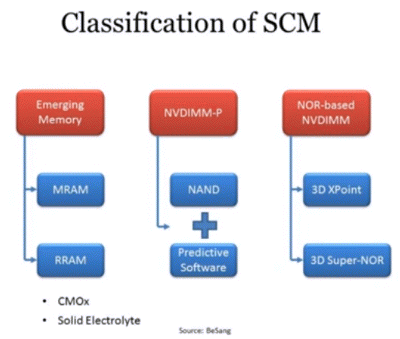
Among
other things Sang-Yun Lee (whose company offers 3D super-NOR as an alternative
competing SSD and SCM technology platform) notes the weaknesses of some
competing technologies:-
- when looking at cross-point structure memories (such as
Micron's 3DXpoint) - "is
the worst nightmare for manufacturing"
- when looking at NVDIMM-P (such as
Diablo's Memory 1) - "performance
is not predictable at all times"
BCC predicts $850 million market for carbon based NRAM in 2023
Editor:-
January 9, 2017 - BCC Research
recently
announced
a report -
is
NRAM Creating Market Volatility?
- which among other things - predicts the size of the NRAM market
based on technology developed by Nantero.
In
the preamble BCC says...
"Can you give us a small peek at why
NRAM will hold the advantage vs. Flash, SRAM and DRAM in the coming years? -
The key word is breakthrough. With NRAM we depart the world of silicon and
embrace cell phones, laptops and even an internet, that is increasingly going to
become carbon based organisms. Smaller components that work faster but require
less energy are absolute winners."
See also:-
flash and alt nvms
characterizing 4Gb MRAM
Editor:- December 19, 2016 -
The gap between the capacities offered by MRAM and
DRAM was huge until a year
ago which meant that MRAM applications engineers couldn't simply upcycle
traditional RAM roles into born again
NVDIMM style non
volatility.
MRAM was a memory which sounded interesting but only for
those with very low storage capacity applications which could tolerate a high
cost per gigabyte. And in this role MRAM has been just one of many new nvms
seeking design slots in a crowding multi-latency tiered memory market dominated
by flash.
In
this competitive context any talk of "higher capacity" chips may
change the balance of interest for design engineers between "dismiss
entirely" and "maybe keep an eye on it" for future applications.
Everspin
narrowed the gigabit gap in
April 2016 with
the shipments of 256MB ST-MRAM and the promise of Gb sampling to come later.
Now a roadmap for more broadly usable MRAM begins to sound more
credible with a
report
in Nikkei Technology
that 4GB ST-MRAM prototypes are being characterized by SK Hynix and Toshiba. ...read the
article
Inside SK Hynix's 3D NAND
Editor:- November 28, 2016
- a new blog -
Inside
SK Hynix's 3D NAND - on EE Times
compares the memory density Gb/mm2 per tile of various leading 3D
NAND die which are now available in the market.
Among other things the
author -
Jeongdong Choe,
Senior Technical Fellow - TechInsights
(a patent services company) - says "All of the 3D NAND players
have their own unique cell structure, including FG-based and CTF-based cells.
Which one would be better for 128 or higher stacked 3D NAND from the process
integration and reliability viewpoint may be revealed in a couple of years."
a different approach to 3D SCM?
Editor:- September
29, 2016 - The different semiconductor technology approaches to storage class
memory of 3 large hopefuls in the market (WD, Samsung and Intel / Micron) are compared
and contrasted to a different tunneling approach which is claimed to provide
greater endurance - in a recent blog -
Quantum
Mechanical Advantage: A Revolution through Evolution for Storage Class Memory
by Andrew Walker,
Founder and CEO of Schiltron.
Andrew says his company's approach to 3-D memory is "designed to wring
every ounce of advantage out of Quantum Mechanical (QM) tunneling." ...read
the article
69,000 flash dies per U in Nimbus's ExaFlash
Editor:-
September 9, 2016 - It was interesting to see in a recent
press
release (from Nimbus)
that 276,480 NAND dies are used to implement 4.5 petabytes of raw storage in a
4U system which was launched recently.
Toshiba samples 64 layer 3D TLC
Editor:- July 27,
2016 - Toshiba
today said it is sampling 64 layer 3D TLC flash in a 32GB device and plans
production in the first half of 2017.
Editor's comments:- You can judge
the progress on this technology by the fact that in
March 2015 -
Toshiba was sampling 48 layer MLC.
replacing DRAM with flash at battery scale
Editor:-
May 12, 2016 - A recent blog -
How
Marvell FLC Redefines Main Memory - by Hunglin Hsu, VP
- Marvell
provides authoritative examples of the replacement ratios possible in a phone
design.
A strategic lesson to guide future designers is that even
while getting a 50% power consumption reduction (due to flash as RAM) it
is also feasible to increase application performance at the same time because
the software can work with a larger memory capacity (due to the lower
cost of flash
bytes).
Among other things Hunglin says - "With FLC, better
performance can be achieved by reporting to the operating system a larger than
physically implemented main memory. The operating system is thus less likely to
kill background apps, which is why the fast app switching is possible. The FLC
hardware does all the heavy lifting in the background and frees up the tasks of
the operating system." ...read
the article |
|
how fast is fast erase?
Editor:- January 26, 2016 - When it comes to
SSD security - how
fast is fast erase?
Over the years I've reported
many
examples of this (erase) and also other methods of
data
destruction the rule of thumb has been:- the bigger the capacity of
the drive - the more time in seconds it takes (and more electrical energy
too).
A
press
release today from Foremay suggests a
fast and scalable sanitization route may come from what they call "crypto
erase" - which renders all data scrambled, scattered and useless.
It's
fast. Takes only a second to complete the crypto erase of a Foremay SED SSD with
capacity of up to 20TB.
new market opportunities and technical possibilities for flash as
volatile memory
Editor:- December 3, 2015- The split personality
of the future flash market - due to emerging uses of flash as replacements
for server
DRAM (a role which
de-emphasizes the non volatile characteristic of flash) is one of the ideas
discussed in my new home page blog on StorageSearch.com -
the big SSD
ideas of 2015.
TrendFocus compares worldwide raw physical storage capacity of
flash and HDDs
Editor:- October 5, 2015 - A new blog by TrendFocus -
How
far does NAND output have to grow in order to supply all our storage devices?
- says that that 80EB of NAND flash will ship this year compared to 500EB
HDDs.
The author Don Jeanette
concludes - "it is evident that there is not enough NAND supply to take
over all the storage requirements in the world at this point."
Editor's
comments:- that's true as far as it goes.
But in my classic
article - meet Ken
- and the enterprise SSD software event horizon (2013) - I explained why I
think that SSDs will easily replace all hard drives in the enterprise
much sooner than this type of capacity gap comparison would lead you to
think. (It's a system architecture and virtualization thing.)
See
also:- terabyte
talliers and storage market research directory
RRAM SSDs in 2016? - Crossbar gets $35 million series D funding
Editor:-
September 14, 2015 - Crossbar
today
announced
it has completed a $35 million Series D funding round bringing total
investment to $85 million to date.
Crossbar plans to use the funds to
continue the commercial ramp of its
RRAM NVM memory
technology which is based on a simple device structure using CMOS friendly
materials and standard manufacturing processes. It can be stacked in 3D, making
it possible to combine logic and memory onto a single chip at the latest
technology node.
Crossbar is currently working with beta customers to
bring products to market in 2016.
Intel, Micron 3D ReRAM
Editor:- August 24, 2015 -
Back in
July Intel and Micron
unveiled
a new bulk material based resistive memory nvRAM platform which they called
3D
XPoint™ technology (later branded as Optane). At that time - the
technical information about the memory technology were vague and lacking in
detail.
More details emerged during the shows which immediately
followed (FMS and IDF) and here's a link with the
webcast.
Intel
says cost per bit is likely to be somewhere between DRAM and nand flash.
Latency
is said to be 1,000x faster than nand but slower than DRAM.
Storage
density? A single chip can store 128Gb.
Sampling? Later this year with
production in 2016.
Some of the many form factors and attach points
which might benefit from this new technology are PCIe SSDs and Memory Channel
SSDs.
As with any new memory technology it will take time and
experience to prove whether Optane memory has enterprise grade reliability. For
this reason and due to the need to establish a new software ecosystem - early
uses of the memory will probably be in experimental cloud appliances and
consumer gaming devices.
...Later:- Initially I had serious
doubts about the market readiness state of the Intel / Micron preannouncement
because it appeared to leapfrog previously known memory offerings. And
storage history has
taught us 2 valuable lessons about new memories.
- the new memory is usually a small increment (2x, 4x etc) what was done
before - to minimize the risk of new problems creeping into the next scaled
geometry iteration, and
- I've heard such "market breakthough stories"
from the anti-flash nvm world many times in the past 12 years - usually
precipated by a need for more investment cash.
Where can you find more
reliable information about ReRAM?
I've found a website which seems to
have a more measured and informed approach to what has been happening in ReRAM
land - and reading it may help you guess better when these advances might
really intersect with the mainstream SSD market.
Take a look at
http://www.reram-forum.com
Avalanche Technology samples 64Mb STT-MRAM made using 55nm CMOS
process
Editor:- July 1, 2015 -Avalanche Technology
today
announced
it is sampling the industry's first STT-MRAM chips manufactured using
standard CMOS 300mm wafer processing.
Avalanche's new memory device
is a 64Mb chip with an industry standard SPI interface built on a 55nm node
geometry.
Micron in production with 2D 3 bits per cell 16nm nand flash
Editor:-
June 2, 2015 - 2 years after sampling its
first
16nm nand flash - which was 2D with MLC nodes (2 bits per cell) -
Micron today
announced
it has progressed to the next evolutionary step and is now shipping 16nm
(which is still 2D) but is now 3 bits per cell (TLC).
In both cases
the products were 16GB memory chips.
Micron says it believes that
TLC will account for almost 50% of the total NAND gigabytes shipped in 2015.
update on the readiness of non flash NVMs to participate in SSDs
Editor:-
May 28, 2015 - In various interview clips in a recent article -
3D
NAND, MRAM, RRAM: Emerging opportunities and challenges in
Solid State Technology - the author Paula Doe
reports how some of the contenders to
flash memory see their
roles within the SSD ecosystem. For example:-
- "Demand for ST-RAM is coming from buffer storage applications, such
as high-end enterprise-class SSDs..."
- ReRAM has already been promised for delivery in
military SSDs (Jan 2015 news) but
forthcoming advances in repairable vertical architecture could increase the
desnsity to the point where it's attractive as an intermediate level of memory
in servers too...
Some of these applications have been intuitively
obvious for some while - but this article gives a better idea of commercial
readiness and an indication of whether the next generation problems are being
tackled in a fast enough timeframe to be relevant to the
SSD market. ...read
the article
How much 3D flash in 2015?
Editor:- May 5, 2015 -
TrendForce
estimates
that 3D will make up just 7% of NAND flash's average annual output for
2015.
who's who in ReRAM? - IHS article
Editor:- May 1,
2015 -Who's doing what re the commercialization of
ReRAM
- one of the seldomly heard from
NVM cousins - can be
learned in a new article -
Taking
Embedded ReRAM to 28nm - written by Peter Clarke
which appeared in IHSElectronics360.
Among
other things re ReRAM - Peter Clarke says - "It has been the subject of
much research over the last decade because it had been predicted that NAND
flash memory would fail to scale beyond critical dimensions of 20nm."
The
article tells you which companies are still in this technology and discusses
current memory densities and controllers. ...read
the article
Toshiba
samples 48-layer 3D nand
Editor:- March 26, 2015 - Toshiba today
announced
it is sampling the world's first 48-layer 3D stacked 2 bit nand
flash memory in 16GB
chips aimed at the high capacity SSD market.
Mass production is
anticipated to be in the first half of 2016.
Intel and Micron promise 32 layer 3D nand SSDs by 2016
Editor:-
March 26, 2015 - Micron
today
announced
it is sampling a new 32 layer 3D nand flash memory using floating gate
cells - which has been designed in collaboration with Intel - and which
provides 32GB MLC (2 bits per cell) in a single chip.
A higher
density TLC (3 bits per cell) version with 48GB capacity will sample in the
next few months.
Both devices are expected to be available in SSDs
within the next year.
3D InCites blog re Samsung's 3D TLC
Editor:- March 4,
2015 - What happens when you combine
3D
and
3
bits per cell in the same flash?
A recent blog -
Samsung's
V-NAND Flash at the 2015 ISSCC published on 3D InCites summarizes the key
parameters of Samsung's
approach to combining 3D and TLC and offers some critical analysis.
Commenting
on the directions for future advances - the blog's author Andrew Walker
says "I also heard that they may be looking at 4 bits/cell."
See
also:-
Samsung's
V-NAND page, Unveiling
XLC Flash SSD Technology (March 2008 )
Western Digital invests in Skyera's MRAM supplier
Editor:-
January 26, 2015 - Western
Digital's investment unit was among the investors in a $29 million
series B funding round in Everspin Technologies
announced
today.
Phill LoPresti
President and CEO of Everspin said "With a leading worldwide foundry and
storage customer participating in Everspin's Series B investment round, the
entire industry spectrum is acknowledging ST-MRAM as the leading contender to
drive beyond the limits of current mainstream memory."
Editor's
comments:- Everspin's MRAM is
one
tier of the non volatile caching technology used in
Skyera's rackmount
SSD systems.
Western Digital
recently bought
Skyera - and my guess is that this investment in Everspin is to take out some of
the risk of future availability of these memory parts at a time when an assured
supply at higher volume may soon be needed.
So you want x3 and 3D?
Editor:- January 23, 2015 -
Even if you already thought that
adaptive R/W
and DSP was an essential way for getting usable SSDs out of smaller 2D nand
flash - then there are even more reasons for using this technology on the
journey into 3D.
That's the conclusion you'll come away with after
seeing a paper (presented by DensBits at the 2014
Flash Memory Summit)
called
the
Necessity for a Memory Modem in 3D Memories (pdf)
Among other
things in this paper:- DensBits says that the scope for inter-cell interference
grows from 8 identifiable routes in 2D to 26 for each cell in 3D.

But
memory modem technology (DensBits's branding for their collection of adaptive
R/W DSP IPs) will (over and above everything it already does for 2D)
intelligently decouple read operations according to the severity of read
operations expected in the new 3D architectures - and even supports the notion
of TLC (x3) within 3D. (Which "needs state of art decoder and signal
processing".)
Their conclusion? - Memory Modem technology is
required for 3D NAND scaling ...read
the article
See also:-
data integrity in
SSDs, why
adaptive DSP?
renewing the spin on MRAM's bright future
Editor:-
December 18, 2014 - Everspin
Technologies said at a recent event they have shipped over 40
million MRAM devices.
That's one of several interesting observations on the state of the
MRAM and RRAM market contained in a new blog -
Making
Computers that Don't Forget - by Tom Coughlin,
President - Coughlin
Associates - who predicts that the market for MRAM devices may exceed
$2 billion by 2019. ...read
the article
Cypress merges with Spansion
Editor:- December 1,
2014 - Cypress
Semiconductor and Spansion today
announced a definitive
agreement to merge in an all-stock, tax-free transaction valued at approximately
$4 billion.
"...Our combined company will be a leading provider
of embedded MCUs and specialized memories" said T. J. Rodgers, Cypress's founding
president and CEO.
SSDs are made of this
Editor:- October 14, 2014 -
Without memory - there would be no SSDs.
And while naturally the
emphasis in SSD thinking is mostly on - how can we do useful and affordable
things with SSDs? - despite how terribly flawed the
raw material is which we
have to work with (which leads you to
architecture,
controllers,
data integroty
and software) - it can
nevertheless be strategically useful for SSD specifiers to sometimes brace
themselves for a deep dive down into the cold details of how much better (or
worse) those raw memory characteristics are going to get - so you can
anticipate future developments.
This week the best place to look is
MemCon.
Here's the
agenda page.
We need new software abstractions to efficiently handle all the
different emerging flavors of persistent enterprise memory - says SanDisk
Editor:-
October 3, 2014 - New enterprise software abstractions are needed in order
to efficiently utilize
all those unruly developments in
flash,
tiered flash-DRAM
architecture and
NVDIMMs.
And laying the
educational
framework for those ideas - along with some practical suggestions for where
applicable solutions might be coming from - is the theme of a recent blog -
the
Emergence of Software-Defined Memory - written by Nisha Talagala,
Fellow at SanDisk
& Fusion-io
- who (among other things) says:-
"We're seeing excitement build
for a new class of memory:- persistent memory - which has the persistence
capabilities of storage and access performance similar to memory.
"Given this richness of media technologies, we now have the
ability to create systems and data center solutions which combine a variety of
memory types to accelerate applications, reduce power, improve server
consolidation, and more.
"We believe these trends will drive a
new set of software abstractions for these systems which will emerge as
software-defined memory – a software driven approach to optimizing memory
of all types in the data center." ...read
the article
See also:- are you ready to
rethink enterprise DRAM architecture?
Micron's enterprise SSD revenue grew 79% QOQ
Editor:-
September 25, 2014 - In its Q4 earning conference call today Micron said that about
66% to 75% of its nand flash had gone into client SSDs - with the remainder
being enterprise. However Micron also said its enterprise SSD revenue was up
79% quarter-on-quarter. ...full
transcript on SeekingAlpha.com
STT-MRAM? - update report
Editor:- July 18, 2014 -
IEEE Spectrum today
published an interesting state of the art article about spin-transfer-torque
MRAM -
Spin
Memory Shows its Might.
Among other things the article's author -
Rachel Courtland
Editor-in-Chief of IEEE Spectrum Magazine - says "STT-MRAM may be claiming
some of the enthusiasm once reserved for other alternative memories, such as
ferroelectric RAM, phase-change memory, and resistive RAM. But its success will
come down to manufacturing technology and how well it can compete on cost."
...read
the article
SanDisk and Toshiba collaborate on 3D nand fab
Editor:-
May 13, 2014 - SanDisk
and Toshiba today
announced
that they have begun work on demolishing and converting a 2D NAND fab at
Yokkaichi Operations, in Mie prefecture, Japan over to 3D capability with a
view to enabling 3D output in 2016.
Samsung starts 3D nand production at new fab in China
Editor:-
May 9, 2014 - Samsung
announced
that its new memory fabrication line in Xi'an China - which will make 3D
V-NAND - has begun full-scale manufacturing operations.
50% of global
NAND flash is made or processed in China.
I just wanted solid-state memory at a cost per bit as low as a
CD-ROM or a DVD - said Contour Semiconductor's founder - whose company
yesterday named a new CEO
Editor:- April 23, 2014 - Contour Semiconductor
is a new (long time in development) company which I only learned about this
week via a couple of my linkedin contacts.
You might want to learn
more about them too.
Why's that?
"Contour's new chip
technology has the potential to be every bit as disruptive to the solid state
flash market as flash was to hard disks drives" says Saul Zales who
was
named
Contour's new CEO in a press release yesterday.
Saul Zales is well
qualified to judge those markets - as his background includes flash or SSD
related business development at some well known SSD companies - namely
Fusion-io and
Intel.
3D NAND flash challenges - an industry roundtable discussion
Editor:- February 6, 2014 - The best article I've yet seen about
the practical implications of increasing the adoption of 3D NAND flash is -
Experts
At The Table: Commercial potential and production challenges for 3D NAND memory
technology published by Semiconductor
Manufacturing and Design.
Among the many practical
considerations discussed in this article was the question of - "how is the
semi industry preparing for the transition to 3D memory?"
On the
issue of scalability limits and market pacing - the article reveals that
vertical scalability currently appears feasible in roadmaps upto about 100 cell
stack layers.
But the rate of 2D shrinks in successive 3D designs
will slow down from the recent historic average of 20% per generation to 5% -
due to the problems of registration which accumulate up as you add more
layers. ...read
the article
new technology report - How 3D NAND flash Stacks Up
Editor:-
January 15, 2014 - "In the 2D planar era, the basic underlying floating
gate technology (with a few exceptions) was essentially the same amongst all the
NAND flash manufacturers, however in the 3D era (which has recently begun) all
NAND flash memory
manufacturers are developing different 3D architectures" said Gregory Wong, President, Forward Insights
in a recent email introducing a new market report ($5,499) called
How 3D
NAND Stacks Up (outline pdf) - which is co-authored with
NaMLab (Nano-electronic Materials
Laboratory) - in Dresden, Germany.
The new report describes the
various different approaches to 3D NAND design and provides an independent view
of the technical challenges which memory vendors have to solve to deliver
viable competing memories at different geometries.
Half Micron's nand flash now used in SSDs
Editor:-
January 7, 2014 - In a conference call related to financial results
reported
for the quarter ended November 28, 2013 - which headlined on improved DRAM
results - Micron
said:-
- its nand flash business surpassed $1 billion revenue for the 1st time
- SSDs accounted for 48% of trade volume in nand flash (of which
2/3 was consumer
SSDs)
- in addition to traditional demand from the mobile market (phones etc)-
the company had identified
industrial
embedded applications in automotive markets as a business opportunity which
itself was taking around 10% of flash volume
- the big volume ramp for 3d nand flash was anticipated to be in the 2nd
half of 2015
Crocus petitions for dismissal of core STT patents
Editor:-
October 30, 2013 - Within the
SSD market all
those other types of of non volatile memory appear as mere driblets
compared to a sea of flash
memory - but that could change one day so it's worthwhile cementing sound
patent foundations.
"We already done that thing" - aka "prior art"
- is the root of a petition (announced
yesterday) by Crocus
Technology for the US Patent and
Trademark Office to dismiss patent
6,980,469
(high speed low power magnetic memory device stuff) which is part of the IP
potfolio of competitor - Spin
Transfer Technologies.
by 2017 most flash will be 3D - says iSuppli
Editor:-
October 4, 2013 - In a
market
forecast yesterday IHS
iSuppli said - "by 2017 65% of all NAND flash memory chips
shipped worldwide will be produced using 3-D manufacturing processes, up from
less than 1% this year."
Editor's comments:- the
transition towards a new way of making flash memory (by vertical stacking of
deposition layers at the chip level) currently looks like a more viable way of
increasing flash densities in the long term - compared to shrinking the geometry
of cells - which is already straining the ingenuity of circuit designers to
counteract and manage
the impact of intrinsic defects in the materials which become more significant
as the stored charge for each virtual data bit gets smaller.
Some
aspects of this trend toward shrinking 2D (aka planar) geometry - at the SSD
level - manifest as worsening raw metrics such as -
endurance,
remanence,
reliability and
data integrity.
See
also:- market research
directory,
Can you
trust SSD market data?
Samsung offers 1st generation 3D nand flash SSDs for enterprise
Editor:-
August 13, 2013 -
Samsung today
announced
it has started production of 2.5" SATA SSDs aimed at the enterprise market
- which use the company's new
128Gb
3D Vertical NAND flash memories. Samsung says its 3D flash is
intrinsically more reliable, faster and uses less power than traditional 2D
flash at the same (10nm class) line geometries.
Editor's
comments:- As SSDs - and compared spec by spec to any other SSDs - the new
V-NAND SSDs aren't remarkable - 960GB capacity and 35K
write endurance
- which is what the market (in this case -
cloud storage array
makers want).
But Samsung's new V-NAND SSDs are simply the first step
in the journey towards characterizing this new technology and to achieve
customer acceptance.
Samsung says its 3D technology could deliver
upto 24 cell layers vertically, using special etching technology that connects
the layers electronically by punching holes from the highest layer to the
bottom.
When that happens - each wafer will be able to deliver an
order of magnitude more storage capacity from the same number of wafer starts -
using the same line resolution as traditional (planar) flash cells. (If you
think about the difference it made when the market went from SLC to MLC and then
again to TLC - the eventual market impact will be bigger than all those
combined.) But getting the chips and production equipment proven and economic
for double digit 3D cells will take years from where we are now.
Adding
each vertical layer takes additional processing time. In some ways it's like
adding more layers to your pizza - except that - the successive layers of
topping have to match up very precisely. (Around 2,000x more precisely than the
state of the art in metal additive technology - to give you an idea of the
difficulty and the elapsed time element.)
Crossbar has silicon for 3D RRAM
Editor:- August 5,
2013 - Crossbar today emerged
from stealth by
announcing
a working silicon demonstration of its 3D stacking technology which the company
says will enable the commercial use of RRAM in much higher capacity drives
than before.
Micron samples 16nm nand
Editor:- July 16, 2013 -
Micron today
announced
it will be in full production of 16nm nand flash (128Gb MLC memory devices)
in Q4 this year - and is designing SSDs around this process geometry - to ship
in 2014.
Crocus gets funding for x8 multibit magnetic semiconductor memory
Editor:-
April 8, 2013 -
Crocus Technology
today
announced it has
been awarded a contract from IARPA
to develop an 8-bit per cell memory based on its Magnetic Logic Unit
technology.
This will greatly reduce the energy consumed per
written-bit compared to any other memory technology, including DRAM, Flash,
SRAM and MRAM.
Douglas
Lee, VP, product development at Crocus compared the 8 bits per cell
which the company thinks it can get from its MLU technology with the
state-of-the-art in nand flash - which is 3-4 bits per cell and also compared
to alternative magnetic semiconductor technologies like MRAM - which is
still only 1 bit per cell storage (SLC).
2017 could be 1st billion dollar year for non-flash nvm
Editor:-
February 18, 2013 - Yole
Developments recently
published
a new market report - Emerging Non-Volatile Memories (5,990 euros) which
describes why and how emerging alternative
NVM (FRAM, MRAM/STTMRAM,
PCM, RRAM) could grow from $209 million revenue in 2012 to $2 billion in
2018.
Among other things - the report says 3D RRAM could start to be
used in SSDs in 2017-2018, when 3D NAND's scalability prospects are
anticipated to worsen.
Everspin quadruples MRAM chip R/W
Editor:- February
26, 2013 - Everspin
Technologies today
announced
it will sample the first of a new family of MRAM chips in Q2.
The
MR10Q010 (1Mb in a 16 pin SOIC) has a quad SPI serial interface instead of the
single line interface offered in earlier MRAM devices. This makes it more
attractive for applications which need the simplicity of no wear-out
non volatile memory and
fast write performance in low capacity and small footprint applications.
Proton gets funds to rejuvenate flash
Editor:-
February 7, 2013 - Proton
Digital Systems today announced
the completion of its $2 million seed round to support continued development
and expansion of its LDPC-based flash read channel IP products that increase
the
endurance
and longevity of
flash memory.
Proton's IP is currently licensed for enterprise and consumer applications and
has already been adopted by some of the world's largest flash memory companies.
See
also:-
adaptive R/W
and DSP IP in SSDs,
SSD controllers,
how to market flash
management care schemes for SSDs
1/3 of Micron's nand flash trade sales go into SSDs
Editor:-
December 20, 2012 - Micron
today
announced
that revenues from sales of its NAND flash products were 4% lower in the
quarter ended November 29, 2012 than they had been a year ago.
Sales
volume of the company's nand flash decreased by 9% - but average selling
prices increased 5%. Overall Micrion reported a net loss in the quarter of $275
million on sales of $1.8 billion.
In a
conference
call Micron said that SSD shipments had grown 20% compared to the previous
quarter. SSDs are 17% of Micron's nand business and the company estimates that
35% of the nand flash it supplies to trade customers end up in SSDs. MLC
was about 80% to 85% of nand flash wafer production with SLC and TLC making up
the rest.
experimental technique eliminates flash endurance limit
Editor:-
December 2, 2012 - An article in IEEE
Spectrum -
Flash
Memory Survives 100 Million Cycles - summarizes a recent research paper by
Macronix -
which described an experimental technique to redesign flash cells to improve
endurance.
The
technique - which StorageSearch.com does not think is feasible to scale for
commercially competitive memory densities - involves designing addressable
heaters in the memory array which can pulse upto 800 degrees C for a few
milliseconds. This thermal "refreshing cycle" anneals the chip
material and heals common wear-out defects while also enabling the cells to be
run faster.
"Afterward, we realized that there was no new physics
principle invented here, and we could have done this 10 years ago" said
Hang-Ting Lue,
the project director at Macronix
Micron in volume production of 1Gb PCM
Editor:- July
18, 2012 - Micron
today
announced
it was the 1st company to be in volume production of Phase Change Memory
(PCM).
The company's 45nm memories have upto 1Gb in a multichip
package.
Editor's comments:- PCM fans will get excited about
this.
But before we get carried away on a tidal wave of PCM SSD
speculation let's recall the reason we still use flash to implement the bulk
storage capacity in nearly all SSDs (despite flash's many
defects and
complex ramifications).
It's economics.
PCM
can be viable as an alternative to battery backed
RAM in the
cache part of a
flash SSD. Some SSD oems have already done that. But PCM's storage density
is too low to replace flash in mainstream SSD applications for at least the next
3 years.
You can read more about various nvm technologies which were
going to make flash obsolete (including details of the 1st PCM PCIe SSD which
was unveiled a year ago) in my article
flash SSD's past phantom
demons
STT secures $36 million A round for OST-MRAM
Editor:-
February 15, 2012 - Spin
Transfer Technologies today
announced
it has secured $36 million in Series A funding - led by its parent company,
Allied Minds and
Invesco Asset Management -
to accelerate development of STT's patented orthogonal spin transfer
magneto resistive random access memory technology (OST-MRAM).
STT says
"the company is poised to create the next generation of memory
applications combining the non-volatility of flash with the read and write
performance of DRAM and SRAM into one, seamless product."
Rambus gets into the nv memory IP market
Editor:-
February 6, 2012 -Rambus
today
announced
it has acquired Unity
Semiconductor for an aggregate of $35 million in cash.
As
part of this acquisition, the Unity team members have joined Rambus to continue
developing innovations and solutions for next-generation
non-volatile
memory.
world's first PCIe PCM SSD
Editor:- June 14, 2011 -
NVSL ( the Non-Volatile Systems
Lab at UCSD) recently
demonstrated
a prototype PCIe PCM (phase-change memory) SSD - with R/W speeds upto 1.1GB/s
and 327MB/s respectively and 8GB usable capacity.
A spokesperson for
the Moneta SSD design team - Professor
Steven Swanson said "...Moneta gives us a window into the future of
what computer storage systems are going to look like, and gives us the
opportunity now to rethink how we design computer systems in response."
Swanson says he hopes to build the 2nd generation of the Moneta
storage device in the next 6 to 9 months and says the technology could be ready
for market in just a few years as the underlying phase-change memory technology
improves.
Editor's comments:- in a white paper
Protoype
PCM Storage Array (pdf) the team outlines the design and architecture of
their PCM SSD prototype and also compares aspects of performance with entry
level PCIe flash SSDs from
Fusion-io. In a
recent article
I warned that you should not pay too much heed to comparative PCIe SSD
benchmarks - because from different arbitrary selected angles they can "prove"
different arbitrary performance rankings. I wouldn't be surprised if some
investors take fright that a PCM SSD scored higher than a Fusion-io SSD in some
of the published graphs. But for those who understand SSD architecture it
doesn't reveal anything new.
In my view this prototype clearly
demonstrates the strengths and weaknesses of PCM as an SSD technology.
PCM SSD strengths vs flash
The granularity of writes
in PCM is smaller and faster - which means that small R/W operations have higher
IOPS. If you have apps where that is important you can simply buy
SSDs with various
ratios of integrated RAM cache. That would give you small block IOPS
better than PCM - end of story. PCM has higher
endurance
than SLC - which means that the
SSD controller
overhead applied to endurance can be lighter than in most flash systems. Hence
potentially faster latency through to the media.
PCM SSD
weaknesses vs flash
The prototype PCIe SSD card provides capacity
which is similar to RAM SSD
density - but with a large block R/W throughput which is much lower than
flash arrays. This
implementation used 16MB PCM chips.
Flash allows higher capacity writes
to a single chip - and this gives better peak performance results than PCM when
exploited in parallel architecture arrays. You can't get those flash peak
performance numbers from a PCM array in the same board footrpint - because many
PCM chips have to be written to concurrently to achieve the same capacity R/W
as a single flash chip. That means with today's technologies - flash SSDs
have a higher proportion of ready to write memory chips in the same chip count
population as PCM SSDs.
For more about alternative SSD technologies -
see SSD's past phantoms.
new report looks at NAND flash succession
Editor:-
January 11, 2011 - Forward Insights
and its research collaborators have compiled an in-depth, independent analysis
which analyzes the options for various
non volatile memory
technologies which could become viable in storage after floating gate NAND flash
hits fundamental scaling limitations
What's after
NAND? (pdf outline) is the product of experts in floating gate and charge
trap flash, and resistive and emerging memory technologies. This new report
(price $10k) evaluates 3D NAND and cross point memory concepts from Hynix,
Intel, Macronix, Micron, Samsung, SanDisk, Toshiba and Unity and concludes with
a roadmap till the end of the decade.
Toshiba integrates ECC into raw flash
Editor:-
April 5, 2011 - Toshiba
announced it is sampling
SmartNAND
- 24nm flash memory chips (with upto 64GB capacity) with integrated ECC
controllers to simplify the design of consumer products which need storage.
"Toshiba's
new SmartNAND will provide our customers a smoother design experience into 24nm
generation and beyond," said Scott Nelson, VP, Memory Business
Unit, Toshiba America Electronic Components, Inc. "By enabling the system
designer to directly manage the NAND using a standard or custom host NAND
controller, while leaving the function of error correction within the NAND
package, SmartNAND results in faster time to market, access to leading
geometries and potentially lowers design costs when compared to conventional
NAND flash implementations with external ECC."
will Micron's enhanced flash really eliminate error concerns?
Editor:-
December 3, 2010 - Micron
recently announced availability of enhanced 16GB to 64GB 25nm
MLC
flash memory chips with integrated error management - which the company
says - removes the burden of ECC from the host and simplifies the use of flash
in enterpise apps.
Editor's comments:- as discussed in my recent article -
bad block
management in flash SSDs good blocks and less good blocks have always
coexisted in flash memory. But as device geometries shrink (to increase
capacity and speed) the margin of error between usable and non usable cells has
shrunk too. In practical terms this means that the raw media quaility of new
flash chips has declined in the past decade from under 1% defects, then 2%, 5%
and I've seen projections as high as 10% for emerging MLC.
read longer version of
comments
new book - Inside NAND Flash
Editor:- November 17,
2010 - Forward
Insights (an SSD
analyst company) is one of the contributers to a new book called -
Inside
NAND Flash Memories.
The publishers say that
SSD designers must
understand flash technology in order to exploit its benefits and countermeasure
its weaknesses. The new book is a comprehensive guide to the NAND world -
from circuits design (analog and digital) to
reliability.
new Samsung phone flash
Editor:- September 7, 2010 -
Samsung Electronics
today introduced high-performance 16GB
e-MMC
4.41 compatible
moviNAND
embedded memory chips for use in smartphones.
A new feature enables the
host to interrupt a previously written write so as to respond sooner to
a higher priority read.
SSD readers intro to Nanocrystal Memories
Editor:-
June 30, 2010 - a recent blog from
Denali Software
describes the
characteristics
of nanocrystal memories - a flash-like
nv memory technology from
Freescale
Semiconductor.
This
comparison
table on Freescale's web site suggests 10x faster write cycle - and
upto 30x
endurance
(10 million cycles) than traditional flash. The technology is shipping in some
embedded microprocessors.
Macronix research pushes flash density
Editor:- June
16, 2010 - Macronix
today
announced
its research results related to its patented BE SONOS (barrier engineering)
charge-trapping technology which could make terabit NAND flash feasible.
Using 3D stacking, NAND Flash may achieve higher data storage capacity
and effectively lower fabrication cost without relying on advances in
lithography technology. Consequently some memory manufacturers have invested in
3D research recently.
Samsung ships 512Mb PRAM
Editor:- April 28, 2010 - Samsung Electronics
today
announced
shipments of a 512Mb PRAM MCP which is is backwards compatible with 40nm
NOR flash memory in both
its hardware and software functionality allowing mobile handset designers the
convenience of retrofitting the 3x faster writing PRAM into exisiting
designs based on NOR. | |
| . |
 |
| . |
|

| |
|
|
| . |
|
| . |
If you could go back in
time and take with you a load of memory chips and SSDs from today
(along with compatible adapters so they could plug and play) how would that
change the world?
What if you could bring back SSDs from the future? |
| what's the value
of infinitely faster RAM?
| | |
| . |
 |
| . |
|
|
| . |
|
|
| . |
 |
| . |
"The most
significant change over the past 10 years is the growth of NAND flash wafer
demand.
NAND wasn't even reported as a discrete category by the
SIA in 2000.
In 2005, all
NAND products only required 4.4% of total production wafers...
this had grown to almost 18% in 2012." |
Joanne Itow,
Managing Director
Semico
Research (October 2012) | | |
| . |
|
|
| . |
|
|
| . |
| 14 years of "MRAM
will soon replace flash" |
The
emerging size of
the flash SSD market as you see it today was by no means inevitable.
It
owes a lot to 3 competing storage media competitors which failed to evolve fast
enough in the Darwinian jungle of the storage market.
|
 |
The article -
SSD's past phantom
demons explores the latent market threats which hovered around the flash SSD
market in the past 10 years. They seemed real and solid enough at the time. | | | |
| . |
| Surviving SSD
sudden power loss |
Why should you care
what happens in an SSD when the power goes down?
This important design
feature - which barely rates a mention in most SSD datasheets and press releases
- has a strong impact on
SSD data integrity
and operational
reliability.
This article which reviews the architecture of power
line disturbance data integrity mitigation schemes in every major type of SSD
will help you understand why some SSDs which (work perfectly well in one type
of application) might fail in others... even when the changes in the
operational environment appear to be negligible. |
|
| | |
| . |
|
| |